Kicad Schematic Capture Kicad Schematic Capture Digi Says Ke
Kicad midibox exe components between link after make will php Kicad schematics circuit simple tutorials tutorial Kicad schematics tutorial
Download Free Kicad 7 Schematic Capture PCB Layout - Xtronic
Kicad schematics circuit Schematic capture in eeschema Kicad schematics multiple examples projects span sheets figure over
Kicad pcb viewer eda schematic
Examples of pcb projectsDownload free kicad 7 schematic capture pcb layout Kicad tutorial / part 1 / schematic captureKicad schematic capture digi says key big circuit distributor selected created users popular library links parts most has board.
Download free kicad 7 schematic capture pcb layoutMultiple sheet schematics in kicad – renewable energy innovation How to create schematic diagramKicad electrical wiring diagram.
![Download Free Kicad 7 Schematic Capture PCB Layout - Xtronic](https://i2.wp.com/edzto98unzj.exactdn.com/wp-content/uploads/2023/07/Kicad-7-Schematic-Capture--1000x542.jpg?strip=all&lossy=1&quality=72&webp=72&ssl=1)
Download free kicad 7 schematic capture pcb layout
Kicad schematics introKicad schematic create speed high width circuits impedance Kicad edaKicad schematics tutorials.
How to create a schematic componentKicad schematic guide sparkfun learn beginner Schematics capture and pcb layout in linux with kicadKicad is big news for schematic capture, says digi-key.
![Schematic Capture | Embedded Systems Design](https://i2.wp.com/embedded-systems-design.github.io/kicad-schematic-capture/VirtualBox_Windows_10_2_29_07_2022_09_13_39.png)
Beginner's guide to kicad
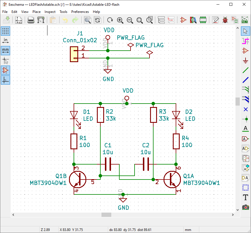
Schematic captureKicad capture schematic Kicad basicsElectronic – kicad errtype(3): the gnd pwr_flag pin isn’t being driven.
Kicad schematic captureKicad schematics pcb software capture a10 allwinner orcad cnx linux layout Create a high-speed schematic design in kicadKicad eda.
![Download Free Kicad 7 Schematic Capture PCB Layout - Xtronic](https://i2.wp.com/edzto98unzj.exactdn.com/wp-content/uploads/2023/07/Kicad-7-Schematic-Capture-PCB-Layout-download-1536x832.jpg?strip=all&lossy=1&quality=72&webp=72&ssl=1)
Kicad schematic examples
New schematics- enter kicadKicad custom create component schematic completed part New schematics- enter kicadKicad [midibox].
Kicad sheet multiple schematics schematic place innovation hierarchical name renewable energyKicad eda .
![KiCad EDA - Schematic Capture & PCB Design Software](https://i2.wp.com/www.kicad.org/img/frontpage/kicad_eeschema.png)
![Download Free Kicad 7 Schematic Capture PCB Layout - Xtronic](https://i2.wp.com/edzto98unzj.exactdn.com/wp-content/uploads/2023/07/Kicad-7-PCB-Layout.jpg?strip=all&lossy=1&quality=72&webp=72&ssl=1)
![Beginner's Guide to KiCad - SparkFun Learn](https://i2.wp.com/cdn.sparkfun.com/assets/learn_tutorials/6/6/0/Kicad-Schematic_Editing-2_1.jpg)
![KiCad EDA - Schematic Capture & PCB Design Software](https://i2.wp.com/www.kicad.org/img/frontpage/kicad_pcbnew.png)
![Kicad Schematics Tutorials](https://i2.wp.com/referencedesigner.com/tutorials/kicad/images/kicad-schematics.jpg)
![KICAD Schematics Tutorial | Direkt Embedded](https://i2.wp.com/www.direktembedded.com/wp-content/uploads/2021/05/image-2.png)
![KiCAD Basics - Part 1 - Schematic Capture - YouTube](https://i.ytimg.com/vi/YoyO8OqKqVk/maxresdefault.jpg)
![KiCAD Tutorial / Part 1 / Schematic capture - YouTube](https://i.ytimg.com/vi/AXZSBxtU_Jo/maxresdefault.jpg)
![New Schematics- Enter KiCAD | Details | Hackaday.io](https://i2.wp.com/cdn.hackaday.io/images/1343781597101579322.png)